Friday, January 8, 2010

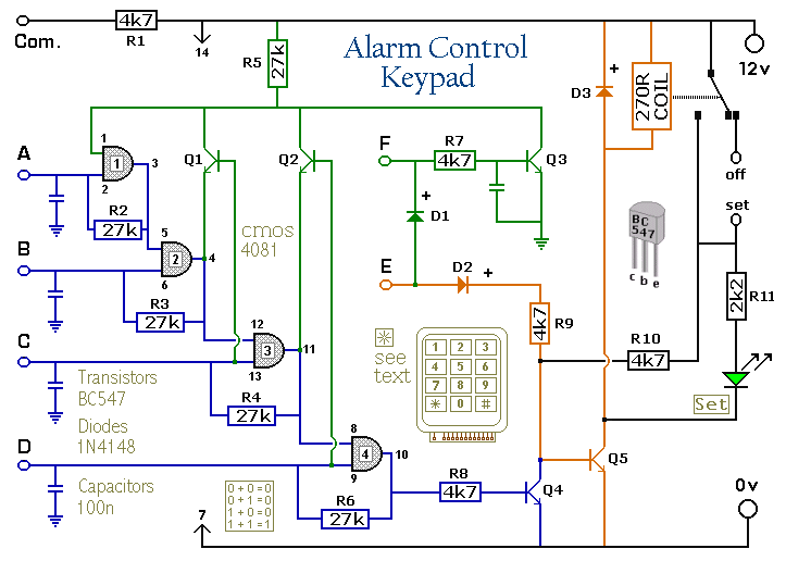
Enhanced 4 Digit Alarm Keypad

Circuit : Ron J
Description:
This is an enhanced 5 digit keypad which may be used with the Modular Alarm System.


4 digit keypad


Notes:
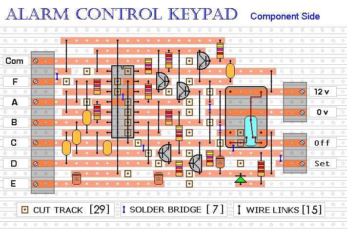
The Keypad must be the kind with a common terminal and a separate connection for each key. On a 12-key pad, look for 13 terminals. The matrix type with 7 terminals will NOT do. The Alarm is set by pressing a single key. Choose the key you want to use and wire it to 'E'. Choose the four keys you want to use to switch the alarm off, and connect them to 'A B C & D'. Your code can include the non-numeric symbols. With a 12-key pad, over 10 000 different codes are available. Wire the common to R1 and all the remaining keys to 'F'. When 'E' is pressed, current through D2 and R9 switches Q5 on. The relay energises, and then holds itself on by providing base current for Q5 through R10. The 12-volt output is switched from the "off " to the "set " terminal, and the LED lights. To switch the Alarm off again it is necessary to press A, B, C & D in the right order. The IC is a quad 2-input AND gate, a Cmos 4081. These gates only produce a high output when both inputs are high. Pin 1 is held high by R5. This 'enables' gate 1, so that when 'A' is pressed, the output at pin 3 will go high. This output does two jobs. It locks itself high using R2 and it enables gate 2 by taking pin 5 high. The remaining gates operate in the same way, each locking itself on through a resistor and enabling its successor. If the correct code is entered, pin 10 will switch Q4 on and so connect the base of Q5 to ground. This causes Q5 to switch off and the relay to drop out. Any keys not wired to 'A B C D or E' are connected to the base of Q3 by R7. Whenever one of these 'wrong' keys is pressed, Q3 takes pin 1 low. This removes the 'enable' from gate 1, and the code entry process fails. If 'C' or 'D' is pressed out of sequence, Q1 or Q2 will also take pin 1 low, with the same result. You can change the code by altering the keypad connections. If you need a more secure code use a bigger keypad with more 'wrong' keys wired to 'F'. A 16-key pad gives over 40 000 different codes. All components are shown lying flat on the board; but some are actually mounted upright. The links are bare copper wires on the component side. Two of the links must be fitted before the IC.

Veroboard Layout


The Support Material for this circuit includes a step-by-step guide to the construction of the circuit-board, a parts list, a detailed circuit description and more.

Tuesday, January 5, 2010

100W RMS Amplifier

100W RMS Amplifier

From: warren@eggo.csee.usf.edu

These materials are provided as-is, with no support. They are not being maintained. At present they are being kept available because we're aware people still refer to them - but we reserve the right to remove this archive, without notice, at any time.

Circuit Description: This is a 100 watt basic power amp that was designed to be (relatively) easy to build at a reasonable cost. It has better performance (read: musical quality) than the standard STK module amps that are used in practically every mass market stereo receiver manufactured today. When I originally built this thing, it was because I needed a 100 WPC amp and didn't want to spend any money. So I designed around parts I had in the shop.
The design is pretty much a standard one, and I'm sure there are commercial units out there that are similar. To my knowlwdge, it is not an exact copy of any commercial unit, nor am I aware of any patents on the topology. To experienced builders: I realize that many improvements and refinements can be made, but the idea was to keep it simple, and should be do-able by anyone who can make a circuit board and has the patience not to do a sloppy job.
The input stage is an LF351 op amp which provides most of the open loop gain as well as stabilizes the quiescent dc voltage. This feeds a level shift stage which references the voltage swing to the (-) rail. The transconductance stage is a darlington, to improve high-frerqency linearity. The 2SC2344 by itself has a rather large collector-base capacitance which is voltage dependent. The MPSA42 presents this with a low-z and has a C(ob) of only a few pf that is effectively swamped by the 33pF pole-splitting cap. The stage is supplied by the 2SA1011 active load (current source) which is about 20 ma. The current to the stage is limited by the 2N3094 to about 70 ma under worst case.
The output is a full complementary darlington with paralleled outputs. Although you could "get away with" only one if only 8 ohm easy-to-drive loads are used, this is not recommended. The use of parallel devices increases the ability to drive reactive loads (which can pull a significant current while the voltage waveform crosses zero and puts a high voltage and a high curent across the transistor simultaneously), gives the amp a higher damping factor, and reduces the maximum current each transistor has to supply to peaks (remember, the gain of a power transistor drops as the current increases).
Compensation is two-pole and one zero. The op-amp's pole and the pole generated by the 33pf cap and the 470 ohm bias resistor of the MPSA42 dominate. (the 33pF gets multiplied by the stage gain.) The 22 pf feedback capacitor provides lead compensation, and is taken from the output of the tranconductance stage rather than the output itself. In this way, the phase lag introduced by the output transistors is not seen by the high-frequency feedback. This intorduces a closed-loop pole which limits the high-frequency response. The two compensation capacitors must be type 1 creamic (NPO) or silver mica - with ZERO voltage coefficient.
The amp was designed to run 2 channels off a +/- 55 volt unregulated supply, reducing to +/- 48 volts under full load. It used a 40-0-40 volt, 5 amp toroid transformer, a bridge rectifier, and 10,000 uf of filter cap per side. If a standard EI transformer is used, a 6-amp rated unit should be used. With this power supply, it produces 100 watts continuous, both channels driven into 8 ohms resistive with no clipping. Dynamic headroom is about a db and a half. For more headroom, unloaded voltages to +/- 62 volts can be used with no circuit modification.
By the way, the schematic is in Postscript.
Limitations:
With no modifications the amp will drive 4-ohm speaker systems with no current limiting. The short-circuit current limit is set to about 4.5 amps peak, which will handle conventional speaker loads.(It will, of course, produce higher peak currents as the output voltage swing approaches the rail.) If you are going to be running some of those high-end speakers with impedance minima of half an ohm, or that stay reactive throughout most of the audio band ( ie, 0.5 +j3.2 ohms) you will probably already own a better amp than this. If the higher-power Motorola power transistors are used, it will drive a 2-ohm resistive load without problems (except heat).
I have never heard any slew-induced distortion on this amp with a CD player's band-limited (22KHz) signal. I suppose that real high-end freaks could pick it to pieces by hitting it with a TTL square wave mixed with a 19KHz stereo pilot tone and crank it up. I guarantee that there will be spurs all over the spectrum, but who listens to that?


Possible Modifications: (What if I want mo' power???) The Toshiba output transistors (2SD424/2SB554 pair) shoud not be used with supply voltages above +/-60 volts. If you plan on cranking it up, use more in parallel or use the 250 watt Motorola pairs (MJ15024/MJ15025). If very low impedances are expected, raise the bias in the transconductance stage to give more base drive to the output darlingtons or add another current gain stage. Higher-Beta (and faster) power transistors can't handle reactive loads worth a crap. Don't substitute high-fT parts unless you are sure they have adequate second-breakdown capability.
The NE5532 op-amp can be used in the input stage. If more than one are used off the +/-15 volt shunt regulators (balanced ins, anti-slew Bessel filters, etc.) the 2.7K dropping resistors may need to be reduced to say, 1.8K ohm to maintain regulation. The 2.7K resistors will allow up to 4 LF351 type op amps off the regulator (I used a quad 347 for balanced inputs to avoid hum in a DJ setup).


Construction tips: The output transistors and thermal compensator (2SC1567) will need to be mounted on a common heat sink - a finned unit measuring 5 in. high by 8 in. wide with 1.25 in fins should do nicely for one channel. (They look nice if you make the sides of the case out of them). Most normal applications won't require more cooling than this. The reason the 2SC1567 was chosen for the output bias regulator is because it is fully insulated - the ECG version will require additional mounting hardware. TO-3 hardware for the outputs is cheap and easy to get.
The driver transistors and voltage amps (2SC3344/2SA1011 pairs) will all require heatsinking as well. Individual TO-220 heat sinks on the circuit board will suffice - the voltage amps dissipate about 1.4 watts each. A common piece of 1/8 in. thick 1 in. wide X 4in. long angle aluminum will suffice for all 4 on each channel, but bear in mind that it must be oriented to take advantage of natural convection, and the transistors must be insualted.
Keep the imput grounds separate from everything else, and return them at ONE point. Failure to do so WILL result in high distortion (5% or so), or even oscillation.
The output stage bias should be set to about 25 milliamps in the output transistors. This value takes a while to stabilize, and you may have to monitor it over an hour or so during initial setup. To measure it, measure the voltage across the emitter resistor and use Ohm's law. This way, you can check the current sharing in the parallel output transistors at the same time and change them if there is a serious discrepancy. With parts of the same date code, they should not be off by more than 10% after it has warmed up. Higher output stage biases can be used, but it takes more care in setting it. If you want an idle current of more than 50 milliamps per side, increase the value of the emitter resistors.


Initial Checkout: DO NOT just plug something like this in! A seemingly insignificant error can set your house on fire! (As well as blow out $30 worth of transistors in a microsecond.) A variac will work in theory, but the amp may latch to the rail if the supply drops too low. I suggest the use of a ballast resistor - a 60 to 100 watt light bulb in series with the AC mains. You get a bright flash when the caps charge, and then it goes (almost) out as the idling supply current reaches its nominal low value. The amplifier will then work normally at low volumes. If the amp draws too much current for whatever reason, the lightbulb will glow brightly, increase resistance, and limit the power to the circuit. Usually, there will either be a mis-wire (use your DMM) or oscillation (will show up on a scope or RF power measuring device). If the bulb goes dim-bright-dim-bright... then the amp is marginally stable and the grounding layout should be checked. Compensation capacitor values may need to be adjusted if any significant changes were made. Mine is stable the way it is.


Additional Notes: The schematic is in postcript, so it should just be able to be printed out. The emitters of the transistors are labelled by an "e". I was too lazy to put arrows on the transistor symbols - and I've been using it that way for over a year now.
Trouble finding parts? MCM (1-800-543-4330) has all the transistors. Total cost for a stereo version should be between $150 and $250, depending on what kind of bargains you can find on the case, transformer, and heatsinks. If you have to pay "list" for everything, it will likely cost about $1000 to build.
The information included herin is provided as-is, with no warranties express or implied. No resposibility on the part of the author is assumed for the technical accuracy of the information given herein or the use or mis-use of said information.
The equipment described in this article was designed, fabricated, and tested on my own personal time using my own personal resources.

Click HERE to get the postscript circuit diagram.

100W Guitar Amplifier Mk II

100W Guitar Amplifier Mk II
Rod Elliott (ESP)
New Version Created 27 Jan 2002
Updated 11 Jan 2008


PCB   Please Note:  PCBs are available for for both power amp and preamp. Click the image for details.

Introduction Guitar amplifiers are always an interesting challenge. The tone controls, gain and overload characteristics are very individual, and the ideal combination varies from one guitarist to the next, and from one guitar to the next. There is no amp that satisfies everyone's requirements, and this offering is not expected to be an exception. The preamp is now at Revision-A, and although the complete schematic of the new version is not shown below, the fundamental characteristics are not changed - it still has the same tone control "stack" and other controls, but now has a second opamp to reduce output impedance and improve gain characteristics.
One major difference from any "store bought" amplifier is that if you build it yourself, you can modify things to suit your own needs. The ability to experiment is the key to this circuit, which is although presented in complete form, there is every expectation that builders will make modifications to suit themselves.
The amp is rated at 100W into a 4 Ohms load, as this is typical of a "combo" type amp with two 8 Ohm speakers in parallel. Alternatively, you can run the amp into a "quad" box (4 x 8 Ohm speakers in series parallel - see Figure 5 in Project 27b, the original article) and will get about 60 Watts. For the really adventurous, 2 quad boxes and the amp head will provide 100W, but will be much louder than the twin. This is a common combination for guitarists, but it does make it hard for the sound guy to bring everything else up to the same level.
Note: This is a fully revised version of the original 100W guitar amp, and although there are a great many similarities, there are some substantial differences - so much so that a new version was warranted. This is (in part) because PCBs are now available for both the power and preamps. The update was sufficiently substantial to warrant retaining the original version, which is still available as Project 27b.
Typical of the comments I get regularly about the P27 power and preamp combo is this e-mail from Tony ...
I'm delighted with the P27B/27 combination. It gives me the clear, punchy, uncluttered sound I've been looking for.

I've grown tired of whistles, bells and other embellishments that some anonymous guitar amp designer somewhere is telling me I've got to have. I've now got the sound I was hoping for. Love the Twin Reverb treble boost. Takes me back to 1960 !!

Without your module/boards and advice I'd have been playing about with breadboards for hours unsuccessfully searching for THE sound. Thanks.
This is just one of many, many e-mails I've received, but manages to sum up most of the comments in a couple of short sentences. This has been a popular project from the beginning, and is a solid and reliable performer that does not sacrifice sound or performance.
Special Warning to all Guitarists

When replacing guitar strings, never do so anywhere near an amplifier (especially a valve amp), nor close to a mains outlet. Because the strings are thin - the top "E" string in particular - they can easily work their way into mains outlets, ventilation slots and all manner of tiny crevices. The springiness of the strings means that they are not easily controlled until firmly attached at both ends. This is very real - click for an image of an Australian mains plug that was shorted out by a guitar string.


The Pre-Amplifier A photo of the Revision-A preamp is shown below. You'll see that there are two dual opamps, but the schematic only shows one. This is the main part of the Rev-A update - the output section now has gain (which is easily selected), and a better buffered low output impedance. The remainder of the circuit is unchanged. Full details of the new version are available on the secure site for those who purchase the PCBs.
photo
Guitar Pre-Amplifier Board (Revision A)
The preamp circuit is shown in Figure 1, and has a few interesting characteristics that separate it from the "normal" - assuming that there is such a thing. This is simple but elegant design, that provides excellent tonal range. The gain structure is designed to provide a huge amount of gain, which is ideal for those guitarists who like to get that fully distorted "fat" sound.
However, with a couple of simple changes, the preamp can be tamed to suit just about any style of playing. Likewise, the tone controls as shown have sufficient range to cover almost anything from an electrified violin to a bass guitar - The response can be limited if you wish (by experimenting with the tone control capacitor values), but I suggest that you try it "as is" before making any changes. (See below for more info.)
Figure 1
Figure 1 - Guitar Pre-Amplifier
From Figure 1, you can see that the preamp uses a dual opamp as its only amplification. The lone transistor is an emitter follower, and maintains a low output impedance after the master volume control. As shown, with a typical guitar input, it is possible to get a very fat overdrive sound by winding up the volume, and then setting the master for a suitable level. The overall frequency response is deliberately limited to prevent extreme low-end waffle, and to cut the extreme highs to help reduce noise and to limit the response to the normal requirements for guitar. If you use the TL072 opamp as shown, you may find that noise is a problem - especially at high gain with lots of treble boost. I strongly suggest that you use an OPA2134 - a premium audio opamp from Texas Instruments (Burr-Brown division), you will then find this quite possibly the quietest guitar amp you have ever heard (or not heard :-). At any gain setting, there is more pickup noise from my guitar than circuit noise - and for the prototype I used carbon resistors!
opamp Notes:
1 - IC pinouts are industry standard for dual opamps - pin 4 is -ve supply, and pin 8 is +ve supply.
2 - Opamp supply pins must be bypassed to earth with 100nF caps (preferably ceramic) as close as possible to the opamp itself.
3 - Diodes are 1N4148, 1N914 or similar.
4 - Pots should be linear for tone controls, and log for volume and master.
The power supply section (bottom left corner) connects directly to the main +/-35V power amp supply. Use 1 Watt zener diodes (D5 and D6), and make sure that the zener supply resistors (R18 and R19, 680 ohm 1 Watt) are kept away from other components, as they will get quite warm in operation. Again, the preamp PCB accommodates the supply on the board.
The pin connections shown (either large dots or "port" symbols) are the pins from the PCB. Normally, all pots would be PCB types, and mounted directly to the board. For a DIY project, that would limit the layout to that imposed by the board, so all connections use wiring. It may look a bit hard, but is quite simple and looks fine when the unit is completed. Cable ties keep the wiring neat, and only a single connection to the GND point should be used (several are provided, so choose one that suits your layout. VCC is +35V from the main supply, and VEE is the -35V supply.
If you don't need all the gain that is available, simply increase the value of R6 (the first 4k7 resistor) - for even less noise and gain, increase R11 (the second 4k7) as well. For more gain, decrease R11 - I suggest a minimum of 2k2 here.
If the bright switch is too bright (too much treble), increase the 1k resistor (R5) to tame it down again. Reduce the value to get more bite. The tone control arrangement shown will give zero output if all controls are set to minimum - this is unlikely to be a common requirement in use, but be aware of it when testing.
The diode network at the output is designed to allow the preamp to generate a "soft" clipping characteristic when the volume is turned up. Because of the diode clipping, the power amp needs to have an input sensitivity of about 750mV for full output, otherwise it will not be possible to get full power even with the Master gain control at the maximum setting.
Make sure that the input connectors are isolated from the chassis. The earth isolation components in the power supply help to prevent hum (especially when the amp is connected to other mains powered equipment).
If problems are encountered with this circuit, then you have made a wiring mistake ... period. A golden rule here is to check the wiring, then keep on checking it until you find the error, since I can assure you that if it does not work properly there is at least one mistake, and probably more.
The input, effects and output connections are shown in Figure 1B.
  • Input - these are quite the opposite of what you might think. The same basic idea is used on Fender amps, as well as nearly all others that have dual inputs for a channel. The Hi input is used for normal (relatively low output) guitar pickups, and is "Hi" gain. "Lo" in this design has about 14 dB less gain, and is intended for high output pickups so the first amplifier stage does not distort. The switching jack on the Hi input means that when a guitar is connected to the Lo input, it forms a voltage divider because the other input is shorted to earth.

  • Effects - Preamp out and power amp in connections allow you to insert effects, such as compression (for really cool sustain, that keeps notes just hanging there), reverb, digital effects units, etc. The preamp out is wired so that the preamp signal can be extracted without disconnecting the power amp, so can be used as a direct feed to the mixer if desired. This is especially useful for bass. The preamp output can also be used to slave another power amplifier (as if you need even more - you do for bass, but not guitar).

  • Output - A pair of output connectors is always handy, so that you can use two speaker boxes (don't go below 4 ohms though), or one can be used for a speaker level DI box. Because of the high impedance output stage, headphones cannot (and must not!) be connected to the speaker outputs. The 'phones will be damaged at the very least, but (and much, much worse) you could easily cause instant permanent hearing loss.
Figure 1b
Figure 1B - Internal Wiring
The connections shown are very similar (ok, virtually identical :-) to those used in my prototype. Noise is extremely low, and probably could have been lower if I had made the amp a little bigger. All connectors must be fully insulated types, so there is no connection to chassis. This is very important !
You will see from the above diagram that I did not include the "loop breaker" circuit shown in the power supply diagram. For my needs, it is not required, for your needs, I shall let you decide. If you choose to use it, then the earth (chassis) connection marked * (next to the input connectors) must be left off.
A few important points ...
  • The main zero volt point is the connection between the filter caps. This is the reference for all zero volt returns, including the 0.1 ohm speaker feedback resistor. Do not connect the feedback resistor directly to the amp's GND point, or you will create distortion and possible instability.
  • The supply for the amp and preamp must be taken directly from the filter caps - the diagram above is literal - that means that you follow the path of the wiring as shown.
  • Although mentioned above, you might well ask why the pots don't mount directly to the PCB to save wiring. Simple really. Had I done it that way, you would have to use the same type pots as I designed for, and the panel layout would have to be the same too, with exactly the same spacings. I figured that this would be too limiting, so wiring it is. The wiring actually doesn't take long and is quite simple to do, so is not a problem.
  • I did not include the "Bright" switch in Figure 1B for clarity. I expect that it will cause few problems.

Bass Guitar, Electric Piano As shown, the preamp is just as usable for bass or electric piano as for rhythm or lead guitar. A couple of changes that you may consider are ...
  • Delete the clipping diodes (unless fuzz bass/piano is something you want, of course). If these are removed, then the output should be taken directly from the Master output pin (M-OUT in Figure 1), so leave out / change the following ...
    • Delete R14, and D1-D4
    • Delete Q1 and associated components (C14, C15, R15, R16, R17)
    • Delete VR5
    • Change R13 from 4.7k to 100 ohms
You may also want to experiment with the tone control caps - I shall leave it to the builder to decide what to change, based on listening tests. C3 and C8 may be increased to 4.7uF to provide an extended bass response. If the gain is too high, simply increase R11 (10k would be a good starting point and will halve the gain).

Power Amplifier The power amp board has remained unchanged since it was first published in 2002. It certainly isn't broken, so there's no reason to fix it. The photo below shows a fully assembled board (available as shown as M27). Using TIP35/36C transistors, the output stage is deliberately massive overkill. This ensures reliability under the most arduous stage conditions. No amplifier can be made immune from everything, but this does come close.
photo
Guitar Power Amplifier Board
The power amp (like the previous version) is loosely based on the 60 Watt amp previously published (Project 03), but it has increased gain to match the preamp. Other modifications include the short circuit protection - the two little groups of components next to the bias diodes (D2 and D3). This new version is not massively different from the original, but has adjustable bias, and is designed to provide a "constant current" (i.e. high impedance) output to the speakers - this is achieved using R23 and R26. Note that with this arrangement, the gain will change depending on the load impedance, with lower impedances giving lower power amp gain. This is not a problem, so may safely be ignored.
Should the output be shorted, the constant current output characteristic will provide an initial level of protection, but is not completely foolproof. The short circuit protection will limit the output current to a relatively safe level, but a sustained short will cause the output transistors to fail if the amp is driven hard. The protection is designed not to operate under normal conditions, but will limit the peak output current to about 8.5 Amps. Under these conditions, the internal fuses (or the output transistors) will probably blow if the short is not detected in time.
Figure 2
Figure 2 - Power Amplifier
Figure 2 shows the power amp PCB components - except for R26 which does not mount on the board. See Figure 1B to see where this should be physically mounted. The bias current is adjustable, and should be set for about 25mA quiescent current (more on this later). The recommendation for power transistors has been changed to higher power devices. This will give improved reliability under sustained heavy usage.
NOTE CAREFULLY As shown, the power transistors will have an easy time driving any load down to 4 ohms. If you don't use the PCB (or are happy to mount power transistors off the board), you can use TO3 transistors for the output stage. MJ15003/4 transistors are very high power, and will run cooler because of the TO-3 casing (lower thermal resistance). Beware of counterfeits though! There are many other high power transistors that can be used, and the amp is quite tolerant of substitutes (as long as their ratings are at least equal to the devices shown). The PCB can accommodate Toshiba or Motorola 150W flat-pack power transistors with relative ease - if you wanted to go that way. TIP3055/2966 or MJE3055/2955 can also be used for light or ordinary duty.
At the input end (as shown in Figure 1B), there is provision for an auxiliary output, and an input. The latter is switched by the jack, so you can use the "Out" and "In" connections for an external effects unit. Alternatively, the input jack can be used to connect an external preamp to the power amp, disconnecting the preamp.
The speaker connections allow up to two 8 Ohm speaker cabinets (giving 4 Ohms). Do not use less than 4 ohm loads on this amplifier - it is not designed for it, and will not give reliable service!
All the low value (i.e. 0.1 and 0.22 ohm) resistors must be rated at 5W. The two 0.22 ohm resistors will get quite warm, so mount them away from other components. Needless to say, I recommend using the PCB, as this has been designed for optimum performance, and the amp gives a very good account of itself. So good in fact, that it can also be used as a hi-fi amp, and it sounds excellent. If you were to use the amp for hi-fi, the bias current should be increased to 50mA. Ideally, you would use better (faster / more linear) output transistors as well, but even with those specified the amp performs very well indeed. This is largely because they are run at relatively low power, and the severe non-linearity effects one would expect with only two transistors do not occur because of the parallel output stage.
Make sure that the bias transistor is attached to one of the drivers (the PCB is laid out to make this easy to do). A small quantity of heatsink compound and a cable tie will do the job well. The diodes are there to protect the amp from catastrophic failure should the bias servo be incorrectly wired (or set for maximum current). All diodes should be 1N4001 (or 1N400? - anything in the 1N400x range is fine). A heatsink is not needed for any of the driver transistors.
The life of a guitar amp is a hard one, and I suggest that you use the largest heatsink you can afford, since it is very common to have elevated temperatures on stage (mainly due to all the lighting), and this reduces the safety margin that normally applies for domestic equipment. The heatsink should be rated at 0.5° C/Watt to allow for worst case long term operation at up to 40°C (this is not uncommon on stage).
Make sure that the speaker connectors are isolated from the chassis, to keep the integrity of the earth isolation components in the power supply, and to ensure that the high impedance output is maintained.

Power Supply WARNING - Do not attempt construction of the power supply if you do not know how to wire mains equipment.
The power supply is again nice and simple, and does not even use traditional regulators for the preamp (details are on the preamp schematic in Figure 1). The power transformer should be a toroidal for best performance, but a convention tranny will do just fine if you cannot get the toroidal.
NOTE Do not use a higher voltage than shown - the amplifier is designed for a maximum loaded supply voltage of +/-35V, and this must not be exceeded. Normal tolerance for mains variations is +/-10%, and this is allowed for. The transformer must be rated for a nominal 25-0-25 volt output, and no more. Less is Ok if the full 100W is not needed.
Figure 3
Figure 3 - Power Supply
The transformer rating should be 150VA (3A) minimum - there is no maximum, but the larger sizes start to get seriously expensive. Anything over 250VA is overkill, and will provide no benefit. The slow-blow fuse is needed if a toroidal transformer is used, because these have a much higher "inrush" current at power-on than a conventional transformer. Note that the 2 Amp rating is for operation from 220 to 240 Volt mains and as shown is suitable for a 200VA transformer - you will need an 4 or 5 Amp fuse here for operation at 115 Volts. Smaller transformers can use a smaller fuse - I am using a 2A slow blow fuse in my prototype (160VA transformer at 240V mains input), which seems to be fine - it allows for a maximum load of 480VA which will never be achieved except under fault conditions.
Use good quality electrolytics (50V rating, preferably 105°C types), since they will also be subjected to the higher than normal temperatures of stage work. The bridge rectifier should be a 35 Amp chassis mount type (mounted on the chassis with thermal compound).
The earth isolation components are designed to prevent hum from interconnected equipment, and provide safety for the guitarist (did I just hear 3,000 drummers asking "Why ??"). The 10 Ohm resistor stops any earth loop problems (the major cause of hum), and the 100nF capacitor bypasses radio frequencies. The bridge rectifier should be rated at least 5A, and is designed to conduct fault currents. Should a major fault occur (such as the transformer breaking down between primary and secondary), the internal diodes will become short circuited (due to the overload). This type of fault is extremely rare, but it is better to be prepared than not.
Another alternative is to use a pair of high current diodes in parallel (but facing in opposite directions). This will work well, but will probably cost as much (or even more) than the bridge.
All fuses should be as specified - do not be tempted to use a higher rating (e.g. aluminium foil, a nail, or anything else that is not a fuse). Don't laugh, I have seen all of the above used in desperation. The result is that far more damage is done to the equipment than should have been the case, and there is always the added risk of electrocution, fire, or both.
Electrical Safety
Once mains wiring is completed, use heatshrink tubing to ensure that all connections are insulated. Exposed mains wiring is hazardous to your health, and can reduce life expectancy to a matter of a few seconds !
Also, make sure that the mains lead is securely fastened, in a manner acceptable to local regulations. Ensure that the earth lead is longer than the active and neutral, and has some slack. This guarantees that it will be the last lead to break should the mains lead become detached from its restraint. Better still, use an IEC mains connector and a standard IEC mains lead. These are available with integral filters, and in some cases a fuse as well. A detachable mains lead is always more convenient than a fixed type (until your "roadie" loses the lead, of course. You will never do such a thing yourself :-)
The mains earth connection should use a separate bolt (do not use a component mounting bolt or screw), and must be very secure. Use washers, a lock washer and two nuts (the second is a locknut) to stop vibration from loosening the connection.

Testing If you do not have a dual output bench power supply
Before power is first applied, temporarily install 22 Ohm 5W wirewound "safety" resistors in place of the fuses. Do not connect the load at this time! When power is applied, check that the DC voltage at the output is less than 1V, and measure each supply rail. They may be slightly different, but both should be no less than about 20V. If widely different from the above, check all transistors for heating - if any device is hot, turn off the power immediately, then correct the mistake.
If you do have a suitable bench supply
This is much easier! Do not connect a load at this time. Slowly advance the voltage until you have about +/-20V, watching the supply current. If current suddenly starts to climb rapidly, and voltage stops increasing then something is wrong, otherwise continue with testing. (Note: as the supply voltage is increased, the output voltage will fluctuate initially, then drop to near 0V at a supply voltage of about +/-15V or so. This is normal.)
Once all is well, connect a speaker load and signal source (still with the safety resistors installed), and check that suitable noises (such as music or tone) issue forth - keep the volume low, or the amp will distort badly with the resistors still there if you try to get too much power out of it.
If the amp has passed these tests, remove the safety resistors and re-install the fuses. Disconnect the speaker load, and turn the amp back on. Verify that the DC voltage at the speaker terminal does not exceed 100mV, and perform another "heat test" on all transistors and resistors.
When you are satisfied that all is well, set the bias current. Connect a multimeter between the collectors of Q10 and Q11 - you are measuring the voltage drop across the two 0.22 ohm resistors (R20 and R21). The desired quiescent current is 25mA, so the voltage you measure across the resistors should be set to 11mV +/-2mV. The setting is not overly critical, but at lower currents, there is less dissipation in the output transistors. Current is approximately 2.2mA / mV, so 10mV (for example) will be 22mA.
After the current is set, allow the amp to warm up, and readjust the bias when the temperature stabilises. This may need to be re-checked a couple of times, as the temperature and quiescent current are slightly interdependent. When you are happy with the bias setting, you may seal the trimpot with a dab of nail polish.
NOTENote: If R22 gets hot or burns out, the amplifier is oscillating! This is invariably because of poor layout, inadequate (or no) shielding between preamp and power amp, or use of unshielded leads for the amplifier input. Please see the photos of my completed amp to see how it should be laid out.

Please see Project 27B for the box designs and other useful info. Click here to see photos of the new amp
10 Watt Power Amplifier

10 Watt Power Amplifier
16

Transistors:
Tr1 BCY70 (or BC 182L or BC212L or BC214L)
Tr2/3/4 BFY50/51
Tr5 BFX88
Tr6/7 2N3055
Risk of instability if no input connected. When testing, connect R (about 3k3). Needs well smoothed power supply of about 20 to 30 volts. Peak power is well over 10 Watts.
The table below shows the approximate voltages to be expected when using a 24v supply and with the variable resistor set to give a current of about 40mA in the output stage.
Test point
Approximate voltage
Tr1(e)
12·5
Tr1(c)
0·65
Tr2(c)
12·5
Tr3(c)
14·4
Tr4(e)
13·7
Tr5(e)
13·1
Tr5(c)
0·6
Tr7(c)
13·1
Circuit diagram : Component Side

Circuit diagram : Copper Side

Acknowledgements : The 10W amplifier is taken from "Transistor Audio and Radio Circuits" published by Mullard.

Friday, January 1, 2010

60W Bass Amplifier

60W Bass Amplifier


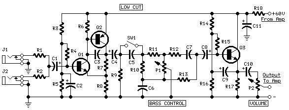
Low-cut and Bass controls
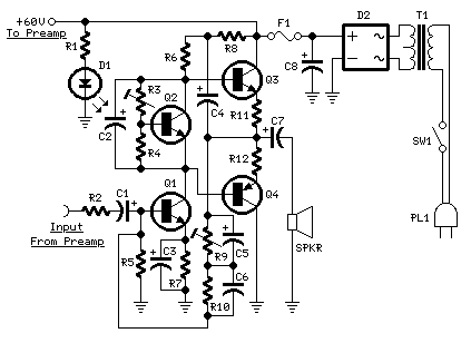
Output power: 40W on 8 Ohm and 60W on 4 Ohm loads

Amplifier circuit diagram:


60W Guitar Amplifier


Amplifier parts:

R1__________________6K8    1W Resistor
R2,R4_____________470R   1/4W Resistors
R3__________________2K   1/2W Trimmer Cermet
R5,R6_______________4K7  1/2W Resistors
R7________________220R   1/2W Resistor
R8__________________2K2  1/2W Resistor
R9_________________50K   1/2W Trimmer Cermet
R10________________68K   1/4W Resistor
R11,R12______________R47   4W Wirewound Resistors

C1,C2,C4,C5________47µF   63V Electrolytic Capacitors
C3________________100µF   25V Electrolytic Capacitor
C6_________________33pF   63V Ceramic Capacitor
C7_______________1000µF   50V Electrolytic Capacitor
C8_______________2200µF   63V Electrolytic Capacitor (See Notes)

D1_________________LED    Any type and color
D2________Diode bridge   200V 6A

Q1,Q2____________BD139    80V 1.5A NPN Transistors
Q3_____________MJ11016   120V 30A NPN Darlington Transistor (See Notes)
Q4_____________MJ11015   120V 30A PNP Darlington Transistor (See Notes)

SW1_______________SPST Mains switch

F1__________________4A Fuse with socket

T1________________220V Primary, 48-50V Secondary 75 to 150VA Mains transformer

PL1_______________Male Mains plug

SPKR______________One or more speakers wired in series or in parallel
                  Total resulting impedance: 8 or 4 Ohm
                  Minimum power handling: 75W


Preamplifier circuit diagram:


Bass Preamp


Preamplifier parts:

P1_________________10K   Linear Potentiometer
P2_________________10K   Log. Potentiometer

R1,R2______________68K   1/4W Resistors
R3________________680K   1/4W Resistor
R4________________220K   1/4W Resistor
R5_________________33K   1/4W Resistor
R6__________________2K2  1/4W Resistor
R7__________________5K6  1/4W Resistor
R8,R18____________330R   1/4W Resistors
R9_________________47K   1/4W Resistor
R10________________18K   1/4W Resistor
R11_________________4K7  1/4W Resistor
R12_________________1K   1/4W Resistor
R13_________________1K5  1/4W Resistor
R14,R15,R16_______100K   1/4W Resistors
R17________________10K   1/4W Resistor

C1,C4,C8,C9,C10____10µF   63V Electrolytic Capacitors
C2_________________47µF   63V Electrolytic Capacitor
C3_________________47pF   63V Ceramic Capacitor
C5________________220nF   63V Polyester Capacitor
C6________________470nF   63V Polyester Capacitor
C7________________100nF   63V Polyester Capacitor
C11_______________220µF   63V Electrolytic Capacitor

Q1,Q3____________BC546    65V 100mA NPN Transistors
Q2_______________BC556    65V 100mA PNP Transistor

J1,J2___________6.3mm. Mono Jack sockets

SW1_______________SPST Switch


Circuit description:
This design adopts a well established circuit topology for the power amplifier, using a single-rail supply of about 60V and capacitor-coupling for the speaker(s). The advantages for a guitar amplifier are the very simple circuitry, even for comparatively high power outputs, and a certain built-in degree of loudspeaker protection, due to capacitor C8, preventing the voltage supply to be conveyed into loudspeakers in case of output transistors' failure.
The preamp is powered by the same 60V rails as the power amplifier, allowing to implement a two-transistors gain-block capable of delivering about 20V RMS output. This provides a very high input overload capability.

Technical data:
Sensitivity:
70mV input for 40W 8 Ohm output
63mV input for 60W 4 Ohm output

Frequency response:
50Hz to 20KHz -0.5dB; -1.5dB @ 40Hz; -3.5dB @ 30Hz

Total harmonic distortion @ 1KHz and 8 Ohm load:
Below 0.1% up to 10W; 0.2% @ 30W

Total harmonic distortion @ 10KHz and 8 Ohm load:
Below 0.15% up to 10W; 0.3% @ 30W

Total harmonic distortion @ 1KHz and 4 Ohm load:
Below 0.18% up to 10W; 0.4% @ 60W

Total harmonic distortion @ 10KHz and 4 Ohm load:
Below 0.3% up to 10W; 0.6% @ 60W

Bass control:
Fully clockwise = +13.7dB @ 100Hz; -23dB @ 10KHz
Center position = -4.5dB @ 100Hz
Fully counterclockwise = -12.5dB @ 100Hz; +0.7dB @ 1KHz and 10KHz

Low-cut switch:
-1.5dB @ 300Hz; -2.5dB @ 200Hz; -4.4dB @ 100Hz; -10dB @ 50Hz
Notes:

  • The value listed for C8 is the minimum suggested value. A 3300µF capacitor or two 2200µF capacitors wired in parallel would be a better choice.


  • The Darlington transistor types listed could be too oversized for such a design. You can substitute them with MJ11014 (Q3) and MJ11013 (Q4) or TIP142 (Q3) and TIP147 (Q4).


  • T1 transformer can be also a 24 + 24V or 25 + 25V type (i.e. 48V or 50V center tapped). Obviously, the center-tap must be left unconnected.


  • SW1 switch inserts the Low-cut feature when open.


  • In all cases where Darlington transistors are used as the output devices it is essential that the sensing transistor (Q2) should be in as close thermal contact with the output transistors as possible. Therefore a TO126-case transistor type was chosen for easy bolting on the heatsink, very close to the output pair.


  • R9 must be trimmed in order to measure about half the voltage supply from the positive lead of C7 and ground. A better setting can be done using an oscilloscope, in order to obtain a symmetrical clipping of the output waveform at maximum output power.


  • To set quiescent current, remove temporarily the Fuse F1 and insert the probes of an Avo-meter in the two leads of the fuse holder.


  • Set the volume control to the minimum and Trimmer R3 to its minimum resistance.


  • Power-on the circuit and adjust R3 to read a current drawing of about 30 to 35mA.


  • Wait about 15 minutes, watch if the current is varying and readjust if necessary.

100W Audio Amplifier

100W Audio Amplifier


General Description

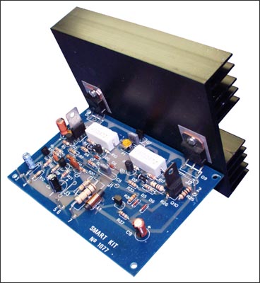
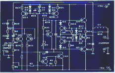
This is an exceptionally well designed amplifier, with a lot of power reserve, high fidelity, low distortion, good S/N ratio, high sensitivity, low consumption and full protection. Having all these almost ideal characteristics this amplifier is likely to become the basic building block of your future high fidelity system, or it can also become the element that will upgrade your existing system.

amplifier25-1.gif
How it Works

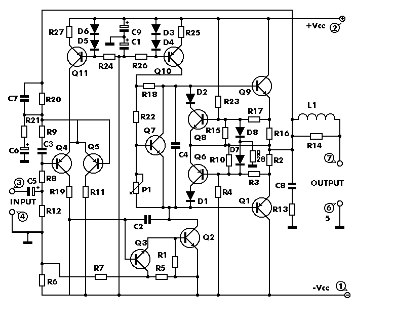
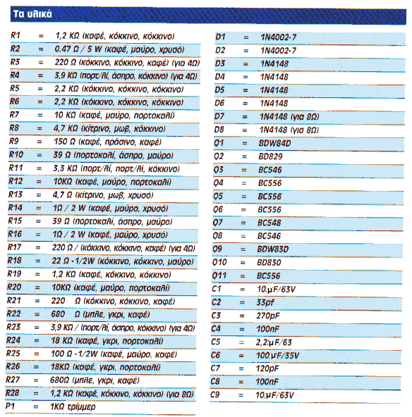
The circuit works from a symmetrical ñ40 VDC power supply and draws a maximum current of 2.6 A. The input circuit of the amplifier is a differential amplifier built around Q4 and Q5 that employ DC feedback thus preventing any DC voltage from appearing across the speaker with the usual destructive results. Q11 acts as a current source and ensures that the input stage draws a constant current of 1 mA. The signal which appears as a voltage drop across the resistor connected in series with the collector of Q4 is used to drive the DARLINGTON pair Q3, Q2 which together with the constant current source of 7 mA that is Q10, form the driver stage. This stage operates in class A and is driving the complementary output stage Q1, Q9. The transistor Q7 is used to balance the circuit at different temperatures and must be mounted on the heatsink between the out put transistors. The feedback loop which consists of R8, R9, C2, C3 provides AC stability to the circuit. The circuit also incorporates a protection stage that makes it virtually indestructible. This protection circuit is built around Q6, Q8. If for whatever reason the output remains connected on one supply rail and the common the output is also protected from high DC voltages that could burn the speakers. The supply rails should be protected by 2 A fuses for the 8 ohm version and 3 A for the 4 ohm.


Technical Specifications - Characteristics

Output power (f=1 KHz, d=0.5 %): 100 W in 8 ohm
Supply voltage: ................ ñ 40 V
Quiescent current: ............. 50 mA
Maximum current: ............... 2.6 A
Sensitivity: . 600 mV
Frequency response: ............ 10-35000 Hz (-1 dB)
Distortion HD: ................. 0.01 %
Intermodulation dist.: ......... 0.02 %
Signal/noise: 83 dBConstruction


PLEASE READ THIS BEFORE YOU START CONSTRUCTION
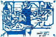
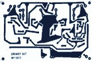
To cater for those who wish to use 4 ohm speakers with this amplifier the Kit includes the necessary components for both versions. The components that differ are R3,4,17 and 23. If you build the 8 ohm version then you must also include in the circuit R28 and D7, D8 which are not used in the 4 ohm version. As you see all the components are already marked on the component side of the p.c. board. The construction is made this way much simpler. Start the construction from the pins and the jumper connections, continue with the resistors and the capacitors and last solder in place the semiconductors. Check each resistor before soldering it, to see if
its colours match those in the component list. Be careful with the electrolytic capacitors because their polarity should be respected. The polarity of those capacitors is marked on their bodies and on the component side of the p.c. board.
NOTE: On the p.c. board next to R2, R16 are marked two other resistors which do not appear in the circuit diagram but are included in the components. They are of 1 ohm 2 W (brown, black, gold) and must be included in the circuit. Take care when you are soldering the semiconductors because if you overheat them they can be damaged. The output transistors should be mounted on the heatsink that is included in the kit. Take care not to short circuit them with the heatsink and we
recommend that you use some HTC between the transistor body and the sink in order to improve heat dissipation. Follow the diagram for the mounting of the power transistors as it shows clearly how to insert the insulators and the screws. Q7 should be made to touch the heatsink and is a good idea to use a bit of HTC between its casing and the surface of the heatsink. When you finish the construction of your project clean the board thoroughly with a solvent to remove all flux residues and make a careful visual inspection to make sure there are no mistakes, components missing and short circuits across adjacent tracks on the board. If everything is OK you can make the following connections: Input: 3 (signal), 5 (common) Output: 7 (signal), 6 (common) Supply: 1 (-40 VDC), 2 (+40 VDC) 5 (0 VDC)

Connect a milliammeter in series with the power supply, short the input of the amplifier, turn the power ON and adjust the trimmer P1 so that the quiescent current is about 50 mA. When you finish this adjustment remove the shunt from the input and connect the output of a preamplifier to it. Connect the pre amplifier to a suitable source and turn everything ON. The signal should be heard from the speakers clear and undistorted. First of all let us consider a few basics in building electronic circuits on a printed circuit board. The board is made of a thin insulating
material clad with a thin layer of conductive copper that is shaped in such a way as to form the necessary conductors between the various components of the circuit. The use of a properly designed printed circuit board is very desirable as it speeds construction up considerably and reduces the possibility of making errors. Smart Kit boards also come pre-drilled and with the outline of the components and their identification printed on the component side to make construction easier. To protect the board during storage from oxidation and assure it gets to you in perfect condition the copper is tinned during manufacturing and covered with a special varnish that protects it from getting oxidised and makes soldering easier. Soldering the components to the board is the only way to build your circuit and from the way you do it depends greatly your success or failure. This work is not very difficult and if you stick to a few rules you should have no problems. The soldering iron that you use must be light and its power should not exceed the 25 Watts. The tip should be fine and must be kept clean at all times. For this purpose come very handy specially made sponges that are kept wet and from time to time you can wipe the hot tip on them to remove all the residues that tend to accumulate on it. DO NOT file or sandpaper a dirty or worn out tip. If the tip cannot be cleaned, replace it. There are many different types of solder in the market and you should choose a good quality one that contains the necessary flux in its core, to assure a perfect joint every time.
DO NOT use soldering flux apart from that which is already included in your solder. Too much flux can cause many problems and is one of the main causes of circuit malfunction. If nevertheless you have to use extra flux, as it is the case when you have to tin copper wires, clean it very thoroughly after you finish your work. In order to solder a component correctly you should do the following:

- Clean the component leads with a small piece of emery paper.  - Bend them at the correct distance from the component body and insert the component in its place on the board.

- You may find sometimes a component with heavier gauge leads than usual, that are too thick to enter in the holes of the p.c. board. In this case use a mini drill to enlarge the holes slightly. Do not make the holes too large as this is going to make soldering difficult afterwards.


- Take the hot iron and place its tip on the component lead while holding the end of the solder wire at the point where the lead emerges from the board. The iron tip must touch the lead slightly above the p.c. board.

- When the solder starts to melt and flow, wait till it covers evenly the area around the hole and the flux boils and gets out from underneath the solder. The whole operation should not take more than 5 seconds. Remove the iron and leave the solder to cool naturally without blowing on it or moving the component. If everything was done properly the surface of the joint must have a bright metallic finish and its edges should be smoothly ended on the component lead and the board track. If the solder looks dull, cracked, or has the shape of a blob then you have made a dry joint and you should remove the solder (with a pump, or a solder wick) and redo it.
- Take care not to overheat the tracks as it is very easy to lift them from the board and break them.
- When you are soldering a sensitive component it is good practice to hold the lead from the component side of the board with a pair of long-nose pliers to divert any heat that could possibly damage the component. 

- Make sure that you do not use more solder than it is necessary as you are running the risk of short-circuiting adjacent tracks on the board, especially if they are very close together.

- When you finish your work cut off the excess of the component leads and clean the board thoroughly with a suitable solvent to remove all flux residues that still remain on it.


amplifier25-3.gif


If it does not work
Check your work for possible dry joints, bridges across adjacent tracks or soldering flux residues that usually cause problems.  Check again all the external connections to and from the circuit to see if there is a mistake there.
- See that there are no components missing or inserted in the wrong places.
- Make sure that all the polarised components have been soldered the right way round. - Make sure the supply has the correct voltage and is connected the right way round to your circuit. 

- Check your project for faulty or damaged components. If everything checks and your project still fails to work, please contact your retailer and the Smart Kit Service will repair it for you.
or

amplifier25-6.gif         amplifier25-7.gif

amplifier25-8.gif
L1 : 10 turns with wire 0,5mm turned on a restistor of 1W
If  you use a 4Ohm speaker you will place R3,4,17,23 at the board.
If you use a 8Ohm speaker you will place D7 D8 and R28.
For R2 and R16 if you don't find a 0,47Ohm place two of 1 Ohm parallel.
R16 must be 0,47Ohm...the 1Ohm must be a typographical error, take care of this, i haven't tested it.

55W (Originally 75W) Power Amplifier

55W (Originally 75W) Power Amplifier

Hugh Dean / Rod Elliott (ESP)
Introduction
This is a contributed project from Hugh Dean in Melbourne, Australia.  Hugh has designed this amplifier for high quality and ease of construction.
Boards
To order boards, click to go to the ESP Purchase form.  Verify the price and postage, then open the order form, fill it in and print it from your browser. Boards are sold only as a stereo pair, and are supplied with component overlay, circuit diagram, bill of materials and assembly and test instructions.  These instructions are as an HTML file on floppy disk.
Kits
Complete kits for this amplifier are available now from the Printed Electronics web site.  For those who do not want to have to scrounge all the component suppliers to get the parts, this is definitely the way to go.  Details and all pricing are available from Printed Electronics - as these may change over time I shall not reproduce them here.
Please Note
According to the latest information on the Printed Electronics web site, the amp has been "downgraded" to 55W, which is still more than enough power for all but the most inefficient loudspeakers.  The maximum recommended supply voltage is +/-35V, and it is recommended that this is not exceeded (the amp was previously stated to use a +/-42V supply voltage).  The drawings below have been duly amended to reflect this change.

Description
From the designer, Hugh Dean ...
The AKSA is a highly refined push pull solid state stereo amplifier of 55W per channel.
It was developed to overcome most of the sonic problems of transistor amplifiers, and incorporates some highly innovative thinking from an experienced designer.  It delivers stunning resolution and a pure, sweet sound at very low cost.
Both channels are assembled on their own individual 86mm x 75mm boards and mounted on a single 300 x 75 mm ledged heatsink.  It is powered from a 35 volt positive and negative supply, and runs very efficiently in Class AB.
Features of this amplifier are its lack of intermodulation and depth of stereo image, unusual for a solid state amplifier.  To achieve the best performance, a dual mono power supply is required - a schematic is supplied with the boards.
To cap it off, the boards are designed so that it can be built up to 100W per channel (into 4 ohms) with only minor changes to various components and the addition of an extra pair of output transistors on each channel.
The complete unit including the power supply can be built up in an afternoon in a suitable case.
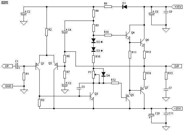
The circuit diagram for the amp is shown in Figure 1.  As can be seen, it is not a complicated amplifier, and all components (excluding power supply) fit onto a single board.
Figure 1
Figure 1 - 75W Power Amplifier
Please Note - The schematic shown is conceptual only, at the request of the designer.  This has been done to protect the design from possible piracy, due to the extremely good performance from what is (or appears to be) a simple circuit.
A full schematic with all component values and assembly instructions is available with the circuit boards.  Normally all ESP projects have complete schematics, but this is not my intellectual property and I will always protect the interests of my contributors.
* The pot (P1) is used to set quiescent current.  This will normally be adjusted to 100mA.  No bias servo is used - instead, the diodes D2 and D3 (1N4148 types) are mounted so that they are in contact with the main heatsink.  These must have their leads insulated and be secured using Superglue to ensure good thermal contact.
All diodes are 1N4148 or 1N914.  Q3 should have a small TO-220 heatsink to prevent overheating.
Apply power (preferably with 22 ohm safety resistors installed in series with the +ve and -ve supply lines) with the pot P1 at minimum resistance - do NOT connect a speaker at this time.  Check for heating of any components, and ensure that the voltage at the output is less than 1 Volt.
To adjust the bias current, reinstall the fuses, do not connect a speaker and apply power.  Wait for a few minutes for the amp to stabilise, then measure the voltage across one of the 0.47 ohm output emitter resistors.  Carefully adjust P1 - when you read a voltage of 47mV, this equates to 100mA.  Verify that the output voltage is within about 100mV.  After a few minutes (checking for heat in the meantime), check the quiescent current again, and adjust as needed.
NOTE: Full schematic, bill of materials, assembly and test instructions are included with each printed circuit board order.

Power Supply
 

WARNING:Mains wiring must be performed by a qualified electrician - Do not attempt the power supply unless suitably qualified.  Faulty mains wiring may result in death or serious injury.
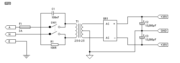
The amp can be operated as a stereo pair form a single supply as shown in Figure 2.  Depending on your needs, this will often be quite adequate.  Note the capacitor and resistor (R1 and C1) across the mains switch.  The capacitor must be rated for at least the full AC supply voltage (i.e. 120V or 240V AC), and all wiring (including the 100 ohm resistor) should be well insulated to prevent accidental contact to the chassis or a finger.  Please read the disclaimer for further suitable warnings about mains wiring.
Figure 2
Figure 2 - Single Power Supply
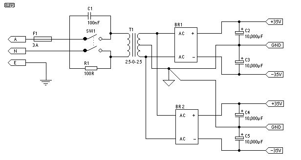
A better solution is to use a "dual-mono" supply.  This shares one transformer, but uses two bridge rectifiers and two sets of filter capacitors.  This arrangement minimises any interaction between the amps, and is shown in Figure 3.  This supply is virtually identical to the one I presented as Project 04 except for the voltage.  Two other differences will be seen if the two are compared - My original supply has an inbuilt "earth-loop breaker" circuit, and this one has an RC "snubber" circuit across the mains switch.  Either of these can be applied on either power supply as required.
Figure 3

300W Subwoofer Power Amplifier

Rod Elliott (ESP)
Introduction
High power amps are not too common as projects, since they are by their nature normally difficult to build, and are expensive.  A small error during assembly means that you start again - this can get very costly.  I recommend that you use the PCB for this amplifier, as it will save you much grief.  This is not an amp for beginners working with Veroboard!
The amplifier can be assembled by a reasonably experienced hobbyist in about three hours.  The metalwork will take somewhat longer, and this is especially true for the high continuous power variant.  Even so, it is simple to build, compact, relatively inexpensive, and provides a level of performance that will satisfy most requirements.
WARNINGS:
  • This amplifier is not trivial, despite its small size and apparent simplicity.  The total DC is over 110V, and can kill you.
  • The power dissipated is such that great care is needed with transistor mounting.
  • The S300 is intended for intermittent duty on 4 Ohm loads, as will normally be found in a subwoofer.  It is NOT intended for PA or any other continuous duty, and although it may work fine for may years, I absolutely do not recommend this.
  • For continuous duty, do not use less than 8 Ohms.
  • There is NO SHORT CIRCUIT PROTECTION.  The amp is designed to be used within a subwoofer enclosure, so this has not been included.  A short on the output will almost certainly destroy the amplifier.
DO NOT ATTEMPT THIS AMPLIFIER AS YOUR FIRST PROJECT

Description
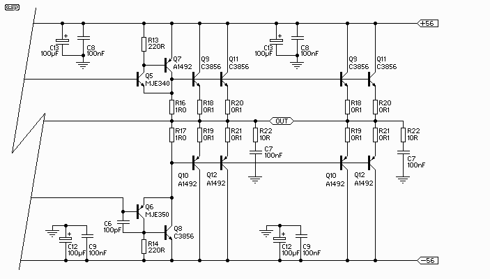
Please note that this amp is NOT designed for continuous high power into 4 Ohms.  It is designed for intermittent duty, suitable for an equalised subwoofer system (for example using the ELF principle - see the Project Page for the info on this circuit).  Where continuous high power is required, another 4 output transistors are needed, wired in the same way as Q9, Q10, Q11 and Q12, and using 0.1 ohm emitter resistors.
Continuous power into 8 ohms is typically over 150W, and it can be used in the form shown at full power into an 8 ohm load all day, every day.  The additional transistors are only needed if you want to do the same thing into 4 ohms!
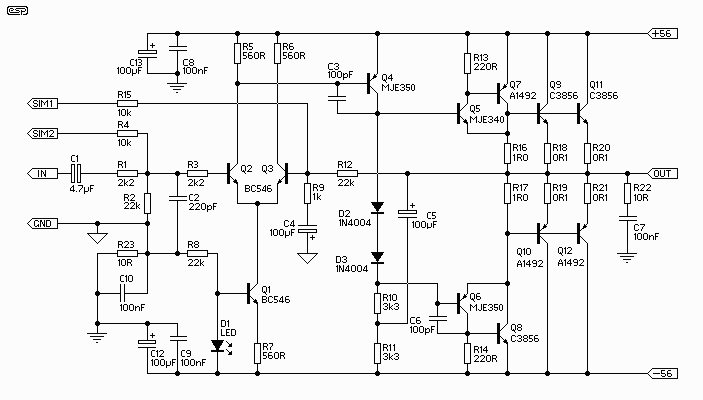
The circuit is shown in Figure 1, and it is a reasonably conventional design.  Connections are provided for the Internal SIM (published elsewhere on the Project Pages), and filtering is provided for RF protection (R1, C2).  The input is via a 4.7uF bipolar cap, as this provides lots of capacitance in a small size.  Because of the impedance, little or no degradation of sound will be apparent.  A polyester cap may be used if you prefer - 1uF with the nominal 22k input impedance will give a -3dB frequency of 7.2Hz, which is quite low enough for any sub.
Figure 1
Figure 1 - Basic Amplifier Schematic
The input stage is a conventional long-tailed pair, and uses a current sink (Q1) in the emitter circuit.  I elected to use a current sink here to ensure that the amp would stabilise quickly upon application (and removal) of power, to eliminate the dreaded turn on "thump".  The amp is actually at reasonably stable operating conditions with as little as +/-5 volts!  Note also that there are connections for the SIM (Sound Impairment Monitor), which will indicate clipping better than any conventional clipping indicator circuit.  See the Project Pages for details on making a SIM circuit.
The Class-A driver is again conventional, and uses a Miller stabilisation cap.  This component should be either a 500V ceramic or a polystyrene device for best linearity.  The collector load uses the bootstrap principle rather than an active current sink, as this is cheaper and very reliable (besides, I like the bootstrap principle :-)
 

All three driver transistors must be on a heatsink, and D2 and D3 should be in good thermal contact with the driver heatsink.  Neglect to do this and the result will be thermal runaway, and the amp will fail.
It is in the output stage that the power capability of this amp is revealed.  The main output is similar to many of my other designs, but with a higher value than normal for the "emitter" resistors (R16, R17).  The voltage across these resistors is then used to provide base current for the main output devices, which operate in full Class-B.  In some respects, this is a "poor-man's" version of the famous Quad "current dumping" circuit, but without the refinements.
Although I have shown 2SC3856 and 2SA1492 output transistors, most constructors will find that these are not as easy to get as they should be.  The alternatives are MJL21193 / MJL21194 or 2SC3281 / 2SA1302 respectively.
Use a standard green LED (do not use high brightness or other colours) - this may be a miniature type if desired.  The resistors are all 1/4W (preferably metal film), except for R10, R11 and R22, which are 1W carbon film types.  All low value resistors (1 ohm and 0.1 ohm) are 5W wirewound types.
Because this amp operates in "pure" Class-B (something of a contradiction of terms, I think), the high frequency distortion will be relatively high, and is unsuited to high power hi-fi.  At the low frequency end of the spectrum, there is lots of negative feedback, and distortion is actually rather good, at about 0.04% up to 1kHz.
Power output into 4 ohms is over 250W continuous, and for transients exceeds 300W easily.  Use of a big power transformer and massive filter caps will allow the amp to deliver close to 350W continuous, but if you really want to use it like that, I very strongly recommend the additional output transistors (see above comments on this topic).
Power Dissipation Considerations
I have made a lot of noise about not using this amp for continuous duty into 4 ohms without the extra transistors.  A quick calculation reveals that at the worst case, the output and transistor voltage will be the same - i.e. at 28V.  With 28V, load (and transistor) current is 7A, so the instantaneous dissipation is therefore 28 * 7 = 196W.  This means that the four final transistors do most of the work, with the others having a relatively restful time.
Since I like to be conservative, I will assume that they contribute no more than about 1.5A (which is about right).  This means that they only dissipate 48W, with the main O/P devices dissipating a peak of 74W each.  The specified transistors are 130W, and the alternatives are 150W, so where is the problem?
The problem is simple - the rated dissipation for a transistor is with a case temperature of 25oC.  As the amp is used, the case gets hot, and the standard derating curves should be applied.  Add to this the reactive component as the loudspeaker drives current back into the amp, and it becomes all to easy to exceed the device dissipation limits.
Figure 1a
Figure 1a - Double Output Stage
Figure 1A shows the doubled output stage, with Q9, Q10, Q11 and Q12 simply repeated - along with the emitter resistors.  Each 1/2 stage has its own zobel network and bypass caps as shown, as this is the arrangement if the dual PCB version is built.  When you have this many power transistors, the amp will happily drive a 4 ohm load all day - with a big enough heatsink, and / or forced cooling (highly recommended, by the way).
A Few Specs and Measurements
The following figures are all relative to an output power of 225W into 4 ohms, or 30V RMS at 1kHz, unless otherwise stated.  Noise and distortion figures are unweighted, and are measured at full bandwidth.  Measurements were taken using a 300VA transformer, with 6,800uF filter caps.
Mains voltage was about 4% low when I did the tests, so power output will normally be slightly higher than shown here if the mains are at the correct nominal voltage.
 
Gain 27dB
Power (Continuous) 240W (4 ohms)

153W (8 ohms)
Peak Power - 5 ms 185W (8 ohms)
Peak Power - 10 ms........ 172W (8 ohms)
Input Voltage 1.3V
Noise -63dBV (ref. 1V)
S/N Ratio 92dB
Distortion 0.4%
Distortion (@ 4W) 0.04% (1 Khz)
Distortion (@ 4W) 0.07% (10 kHz)
Slew Rate > 3V/us
Power Bandwidth 30 kHz
These figures are quite respectable, especially considering the design intent for this amp.  While it would not be really suitable for normal hi-fi, even there it is doubtful that any deficiencies would be readily apparent, except perhaps at frequencies above 10kHz.  While the amp is certainly fast enough (and yes, 3V/us actually is fast enough - full power is available up to 30kHz), the distortion will be a bit too high.
Note that the "peak power" ratings represent the maximum power before the filter caps discharge and the supply voltage collapses.  I measured these at 5 milliseconds and 10 milliseconds.  Performance into 4 ohm loads will not be quite as good, as the caps will discharge faster.  The supply voltage with zero power measured exactly 56V, and collapsed to 50.7V at full power into 8 ohms, and 47.5V at full power into 4 ohms.

Power Supply
 
WARNING: Mains wiring must be performed by a qualified electrician - Do not attempt the power supply unless suitably qualified.  Faulty or incorrect mains wiring may result in death or serious injury.
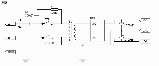
The basic power supply is shown in Figure 2.  It is completely conventional in all respects.  Use a 40-0-40 V transformer, rated at 300VA for normal use.  For maximum continuous power, a 500VA or bigger transformer will be needed.  This will give a continuous power of about 350W, and peak power of close to 400W is possible with a good transformer.  Remember my warnings about using the amp in this way, and the need for the additional output transistors.
Figure 2
Figure 2 - Basic Power Supply Circuit
For 115V countries, the fuse should be 6A, and in all cases a slow blow fuse is required because of the inrush current of the transformer.
C1 must be rated for 240V AC (or 120V AC) operation - do not use standard 250V DC caps under any circumstance, as they will fail, and R1 will explode!  This is not intended as humour - this is fact!  C1 and R1 may be omitted in most cases, and if you cannot get a mains rated capacitor I suggest that you don't install these components.
The supply voltage can be expected to be higher than that quoted at no load, and less at full load. This is entirely normal, and is due to the regulation of the transformer. In some cases, it will not be possible to obtain the rated power if the transformer is not adequately rated.
Bridge rectifiers should be 35A types, and filter capacitors must be rated at a minimum of 63V.  Wiring needs to be heavy gauge, and the DC must be taken from the capacitors  - not from the bridge rectifier.
Although shown with 4,700uF filter capacitors, larger ones may be used.  Anything beyond 10,000uF is too expensive, and will not improve performance to any worthwhile degree.  Probably the best is to use two 4,700uF caps per side (four in all).  This will actually work better than a single 10,000uF device, and will be cheaper as well.
NOTE:  It is essential that fuses are used for the power supply.  While they will not stop the amp from failing (no fuse ever does), they will prevent catastrophic damage that would result from not protecting the circuit from over-current conditions.  Fuses can be mounted in fuseholders or can be inline types.  The latter are preferred, as the supply leads can be kept as short as possible.  Access from outside the chassis is not needed - if the fuses blow, the amplifier is almost certainly damaged.

What Does It Look Like?
I have included a photo of the prototype amp, fully mounted on its heatsink.  For normal use, some brackets would also be needed to mount the heatsink, unless two assemblies were used as the side panels of a conventional (stereo) amplifier chassis.

Figure 3 - Completed Amp Module

Alarms and security related schematics

Audio power amplifier schematics

Audio preamp circuits

Automotive, car and motorcycle schematics

Data acquisition (DAQ) and data logging schematics

Filter schematics

Games and fun stuff (electronic schematics)

Infrared based schematics

LASER related power supplies and data transmission

LED related schematics

Lighting and light controller schematics

Medical and health related schematics

Microcontroller based schematics

Misc audio (also see Music, Amplifiers, Preamp)

Miscellaneous schematics

Models, remote control toys, robotics

Motor and general control schematics

Music related schematics (also see Audio)

PC related schematics

PDA / music player interfaces and schematics

Photography related electronic circuits

Power supplies and control schematics

Radio-frequency schematics (also see Transmitters)

Solar-power schematics

Telephone and intercom related schematics

Test equipment circuit diagrams

Timing and oscillator circuits

Transmitter schematics (also see RF)

Video related circuit schematics